WASSCE Physics · Semiconductors and Electronics
Semiconductors, the p-n diode and rectification
By the WASSCE Tutor team
Updated 10 November 2026 · 6 min read · Prepared against the WASSCE syllabus.
Every phone, radio and solar charger is built on a handful of tiny components made of silicon. Semiconductors conduct better than insulators but worse than metals — and by adding traces of other elements, engineers control exactly how.
Learning objectives
By the end of this lesson you should be able to:
- distinguish conductors, insulators and semiconductors using the idea of free charge carriers
- explain intrinsic and extrinsic (n-type and p-type) semiconductors
- describe the p-n junction diode and its forward and reverse bias
- explain half-wave and full-wave rectification
Conductors, insulators and semiconductors
| Conductors | Semiconductors | Insulators |
|---|---|---|
| many free electrons | few free charge carriers | almost no free charge carriers |
| e.g. copper, aluminium | e.g. silicon, germanium | e.g. glass, rubber, plastic |
| resistance rises with temperature | resistance falls with temperature | very high resistance |
In terms of energy bands: in a conductor the valence and conduction bands overlap; in a semiconductor there is a small energy gap that some electrons can cross when heated; in an insulator the gap is large.
Intrinsic semiconductors
A pure semiconductor (silicon or germanium) is intrinsic. At room temperature, a few electrons gain enough energy to break free of their bonds, leaving behind holes (gaps that behave like positive charges). Both electrons and holes carry current, and they are equal in number. Heating frees more of them, so the resistance falls (the principle of the thermistor).
Extrinsic semiconductors (doping)
Doping is the addition of a tiny, controlled amount of impurity to a pure semiconductor to increase its conductivity.
| n-type | p-type |
|---|---|
| doped with a pentavalent element (5 outer electrons): phosphorus, arsenic, antimony | doped with a trivalent element (3 outer electrons): boron, aluminium, gallium, indium |
| the extra electron is free: electrons are the majority carriers | a missing electron creates a hole: holes are the majority carriers |
| the impurity is a donor | the impurity is an acceptor |
Both types are electrically neutral overall.
The p-n junction diode
When p-type and n-type material are joined, electrons near the junction diffuse into the p-side and fill holes, and holes diffuse the other way. This creates a thin depletion layer with no free carriers, across which a small junction (barrier) potential forms (about 0.6–0.7 V for silicon).
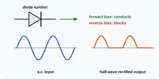
Figure 1. The diode and half-wave rectification. WASSCE Tutor diagram.
- Forward bias: p-side connected to +, n-side to −. The depletion layer narrows; once the p.d. exceeds about 0.6 V, a large current flows.
- Reverse bias: p-side to −, n-side to +. The depletion layer widens; almost no current flows (only a tiny leakage current).
A diode therefore lets current flow in one direction only — the direction of the arrow in its symbol.
Rectification
Rectification is the conversion of alternating current into direct current.
- Half-wave rectification: a single diode in series with the load lets through only the positive half-cycles. The output is a series of humps with gaps.
- Full-wave rectification: a bridge of four diodes (or two diodes with a centre-tapped transformer) turns the negative half-cycles positive too, giving a continuous series of humps.
- Smoothing: a large capacitor across the output charges at the peaks and discharges between them, giving an almost steady d.c.
A phone charger plugged into a 230 V socket contains a small transformer (or switching circuit) to lower the voltage, a bridge rectifier of four diodes, and a smoothing capacitor, giving the steady 5 V d.c. that a phone needs.
Other diodes
- Light-emitting diode (LED): emits light when forward-biased; very efficient; used in indicator lights, torches, LED bulbs and screens.
- Photodiode and solar cell: produce a current when light falls on the junction.
- Zener diode: designed to conduct in reverse at a fixed voltage; used to regulate voltages.
Key points
- Semiconductors (Si, Ge) have resistance that falls with temperature.
- n-type: pentavalent dopant, electrons are majority carriers. p-type: trivalent dopant, holes are majority carriers.
- A p-n diode conducts when forward-biased and blocks when reverse-biased.
- Rectification: half-wave (one diode), full-wave (bridge), smoothed by a capacitor.
WASSCE examination focus
Distinguish n-type and p-type semiconductors (dopants and majority carriers), explain forward and reverse bias of a p-n junction, sketch the I–V characteristic of a diode, and draw circuits and output waveforms for half-wave and full-wave rectification. Explain the role of the smoothing capacitor.
Quick check
- What are the majority charge carriers in an n-type semiconductor?
- In which bias does a diode conduct?
- What is the purpose of a capacitor connected across the output of a rectifier?
Answers: 1. Electrons. 2. Forward bias (p-side to positive). 3. To smooth the output, giving an almost steady d.c.
Keep going with semiconductors and electronics
This is one of 2 lessons in Semiconductors and Electronics. Start free with the first lesson of every topic, then unlock them all, plus exam-style practice marked instantly and guided learning tools, from 25 NLe.
- Free account, no card needed
- Everything from 25 NLe
- No automatic renewal
More lessons in Semiconductors and Electronics
- Transistors, sensor circuits and logic gates🔒